NVIDIA and Cisco Unveil Ultra‑Dense USFP Optics to Double AI Factory Bandwidth
NVIDIA and Cisco announced the Ultra‑Dense Small Form Factor Pluggable (USFP), a 400 Gb/s per lane optical module that lets AI data‑center builders double lane capacity without redesigning existing infrastructure.
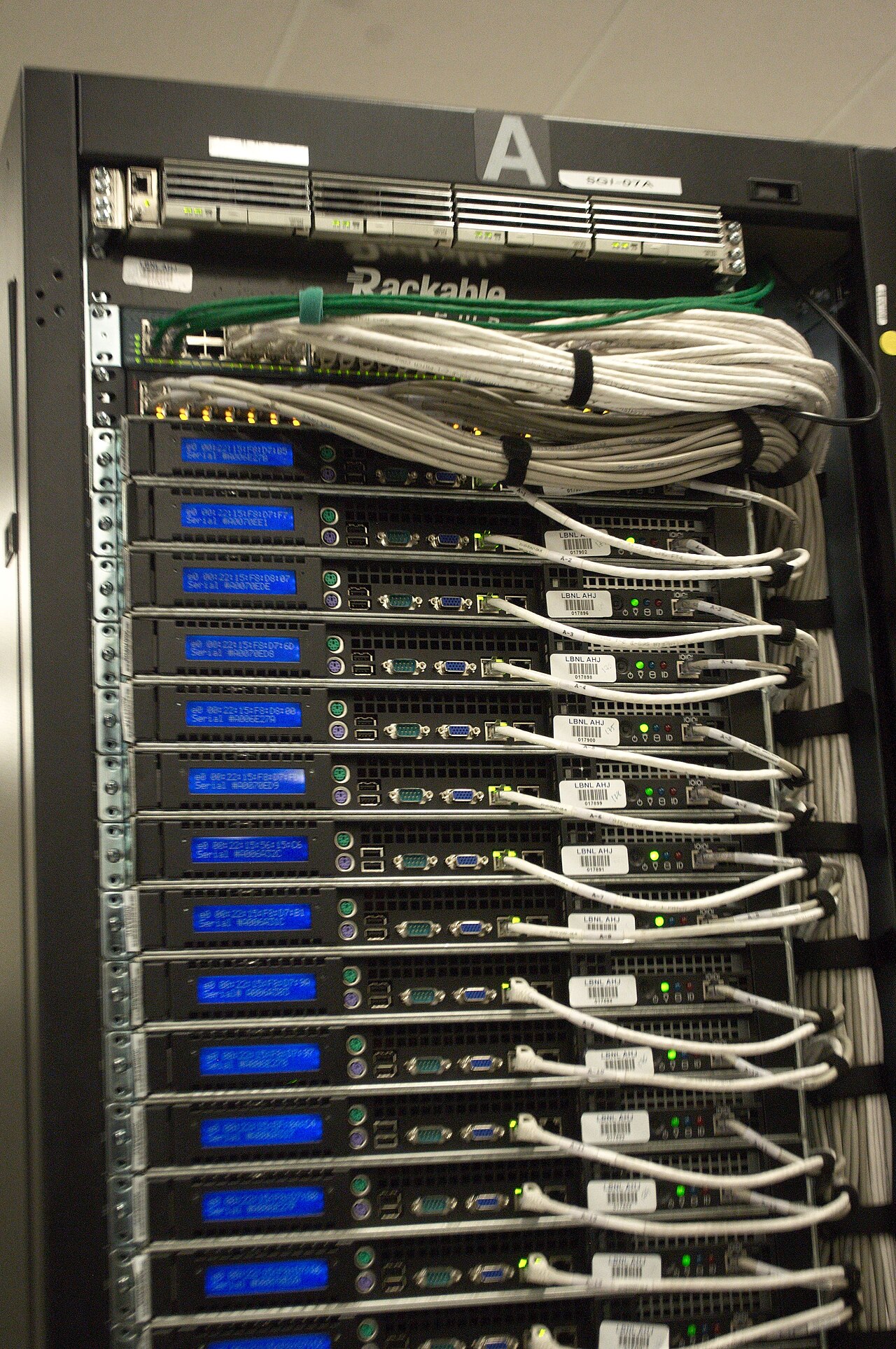
On 12 October 2026 NVIDIA and Cisco presented the Ultra‑Dense Small Form Factor Pluggable (USFP), a new optical transceiver designed specifically for the most demanding AI factories. The announcement highlighted a 400 Gb/s per‑lane data rate, a figure that effectively doubles the 200 Gb/s lane speed that dominates today’s high‑performance compute clusters.
The companies describe USFP as a drop‑in upgrade for existing data‑center racks. According to the joint statement, the module enables AI‑factory builders to move from 200 Gb/s to 400 Gb/s per lane without having to overhaul the surrounding power, cooling or cabling architecture.
Technical specifications and performance claims
The first USFP transceiver will host 16 full‑duplex lanes within a form factor that matches the current OSFP size. Future revisions are planned to support 32 lanes or more, allowing a single module to reach a total throughput of 12.8 Tb/s when each lane carries 1.6 Tb/s of aggregated traffic.
Doubling both lane count and per‑lane bandwidth translates into a front‑panel bandwidth density four times higher than existing 200 Gb/s modules, according to an internal study shared by the partners. The same study also reports an approximate 30 percent improvement in energy efficiency, measured as gigabits per watt, when compared with current 200 Gb/s pluggable optics.
Thermal management is addressed through a 100 W power‑dissipation ceiling that the USFP can handle without a dedicated cooling circuit inside the transceiver. This design choice reduces the overall system complexity and keeps the module’s footprint compatible with existing rack layouts.
Connector innovation and ecosystem development
USFP introduces a two‑dimensional connector that employs a two‑step insertion mechanism. The design reduces contact wear and improves signal integrity, which is essential for maintaining error‑free 400 Gb/s operation across long fiber runs.
Manufacturing partners TE Connectivity and Amphenol will supply the cages, connectors and other mechanical components. Both NVIDIA and Cisco indicated that additional suppliers will join the program as the ecosystem matures, reinforcing the goal of an open, multi‑source specification.
The two companies also announced a plan to create an open‑specification project that will be governed by a community of vendors, researchers and operators. The initiative aims to standardise USFP interfaces, testing procedures and firmware updates, making it easier for data‑center operators to adopt the technology at scale.
- 400 Gb/s per lane data rate
- 16 full‑duplex lanes in OSFP‑sized module (future 32‑lane option)
- Up to 12.8 Tb/s aggregate throughput
- 100 W thermal dissipation without dedicated cooling
Gilad Shainer, senior vice‑president at NVIDIA, summed up the strategic intent: “Building the world’s largest AI factories starts with rethinking the smallest of connections.” The quote underscores the belief that incremental gains at the physical layer can unlock massive scale‑out opportunities for AI workloads.
What this means for English‑speaking organisations
For enterprises and cloud providers that operate AI‑focused data centres, USFP offers a clear path to double lane bandwidth while keeping rack density and power budgets largely unchanged. The higher front‑panel density reduces the number of transceiver slots required per rack, freeing up space for additional compute nodes or storage.
The improved energy efficiency translates into lower operating costs, especially in facilities where power and cooling are already at premium levels. Operators can therefore allocate saved energy to additional workloads or to more aggressive cooling strategies for high‑density GPU clusters.
Because the specification is open, organisations are not locked into a single supplier. This mitigates supply‑chain risk and encourages competitive pricing, a factor that becomes critical when scaling dozens of racks across multiple regions.
In practice, the transition to USFP could allow a typical AI cluster to scale from 6 Tb/s to over 12 Tb/s of inter‑node bandwidth with minimal hardware redesign, accelerating training cycles and enabling more complex models to run in production.
Future roadmap and industry impact
NVIDIA and Cisco indicated that subsequent USFP generations will target even higher per‑lane speeds, potentially reaching 800 Gb/s as silicon photonics matures. This roadmap aligns with the broader industry push toward exascale AI workloads that demand ever‑greater interconnect capacity.
Analysts predict that the USFP form factor could become a de‑facto standard for AI‑centric data centres, prompting rival vendors to develop compatible modules and accelerating the overall pace of optical innovation in the sector.
The announcement also signals a strategic alignment between compute and networking leaders, suggesting that future AI infrastructure will be co‑designed to optimise both silicon performance and the underlying fabric.
Overall, the USFP initiative represents a significant step toward more scalable, efficient, and flexible AI data‑center architectures, positioning NVIDIA and Cisco at the forefront of the next wave of high‑performance networking solutions.
Sources
- Google Actualitésfierce-network.com · October 12, 2026
- HPCwire - Since 1987 – Covering the Fastest Computers in the World and the People Who Run Themhpcwire.com · October 12, 2026